vit-logo

28th IEEE International Symposium on
VLSI Design and Test
(VDAT-2024)
1st - 3rd September 2024
Vellore Institute of Technology, Vellore, INDIA
Emerging Technologies for VLSI Design Ecosystem


vlsi-logo

Tutorial schedule


Forenoon
Time Tutorial 1
(Full Day)
Tutorial 2
(Full Day)
Tutorial 3
(Full Day)
Tutorial 4
(Full Day)
Tutorial 5
(Half Day)
Tutorial 7
(Half Day)
Tutorial 9
(Half Day)
Venue TT 312 Ambedkar Auditorium TT 727 TT 238 Kamaraj Auditorium TT Gallery 2 TT311
Mixed Signal ASIC Design Emerging Technologies VLSI testing and testability (With Hands-on Labs) Design Implementation - (RTL to GDSII Flow with Hands-on Labs) VLSI Design & Reliability System Design Physical Verification
Session-1
09.30 AM to 11.00 AM
Challenges to Backend VLSI Design, Process Flow and Integration

Venkata Reddy Kolagatla,
Shramona Roy ,
and Vivian Desalphine
- C-DAC, Bangalore
Performance-specific, technology look-up table- based design methodology for low-dropout voltage regulators (LDOs) - I.

Sakshi Arora
- IIIT Bangalore
Manikandan R R
- NIT Tiruchirappalli
DFT Fundamentals

Dr. Renold Sam
- Microchip Technology Inc. Canada
Introduction to ASIC Flow & RTL Synthesis

Vijay Kanth,
Mohan Ganugapati
- VLSIMONKS DESIGN PVT LTD
Sreedevi Kulkarni - ChipEdge Technologies Pvt. Ltd.
Life cycle and development of custom Standard cells

Aquib Quraishi
- Marvell Technologies
Energy Efficient VLSI Architectures for DSP: Image and Video Watermarking System on FPGA

Dr. Noor Mohammed
- IIITDM Kancheepuram
Dr. Dhayalakumar M
- Dissai Technologies
Challenges and Solutions during Low Power Mixed Signal (LPMS) SoC Verification

Lalit Mohan
- Cadence Design Systems India Private Limited
Session-2
11.30 AM to 01.00 PM
Digital ASIC Design and Development

Venkata Reddy Kolagatla,
Shramona Roy,
and Vivian Desalphine,
- C-DAC, Bangalore
Performance-specific, technology look-up table- based design methodology for low-dropout voltage regulators (LDOs) - II.

Sakshi Arora
- IIIT Bangalore
Manikandan R R
- NIT Tiruchirappalli
Advanced Fault Modelling Techniques & 3D ICs DFT Design techniques

Yadu Krishnan
- Microchip Technology Inc. India
Floorplanning

Vijay Kanth,
Mohan Ganugapati
- VLSIMONKS DESIGN PVT LTD
Sreedevi Kulkarni - ChipEdge Technologies Pvt. Ltd.
Impact of Design for Test on the production of a Chip

Aanand Venkatachalam,
Suraj MC
- Marvell Technologies
Energy Efficient VLSI Architectures for DSP: Image and Video Watermarking System on FPGA

Dr. Noor Mohammed
- IIITDM Kancheepuram
Dr. Dhayalakumar M
- Dissai Technologies
Design Rules: Concepts, Checking, DRC Aware Place & Route for Custom Flow

Sachin Shrivastava,
Vishal Rastogi,
Deepak Karnatak
- Cadence Design Systems India Pvt. Ltd., Noida
Afternoon
Time Tutorial 1
(Full Day)
Tutorial 2
(Full Day)
Tutorial 3
(Full Day)
Tutorial 4
(Full Day)
Tutorial 6
(Half Day)
Tutorial 8
(Half Day)
 
Venue TT 312 Ambedkar Auditorium TT 727 TT 238 TT Gallery 2 Kamaraj Auditorium
Mixed Signal ASIC Design Emerging Technologies VLSI testing and testability (With Hands-on Labs) Design Implementation - RTL to GDSII Flow (With Hands-on Labs) Internet of Things Design Verification  
Session-1
2.00 PM to 3.30 PM
Analog and Mixed Signal ASIC Design and Development - I

Venkata Reddy Kolagatla,
Shramona Roy, and
Vivian Desalphine
- C-DAC, Bangalore
A Journey across Cryo- CMOS for Quantum Computation - I

Prof. Sudeb Dasgupta
- IIT Roorkee
Prof. Navjeet Bagga
- IIT Bhubaneswar
Lab Session on DFT Synthesis, Scan Insertion, Scan Chain, Analysis, DRC violations analysis and fixing

Prathiba M
- Vellore Institute of Technology, Vellore
Yadu Krishnan
- Microchip Technology Inc. India
Power planning & Placement

Vijay Kanth
Mohan Ganugapati
VLSIMONKS DESIGN PVT LTD
Sreedevi Kulkarni
- ChipEdge Technologies Pvt. Ltd.
Industrial IoT using LoRaWAN Technology

Dr.Subramanian
- Enthu Technology Solutions India Pvt Ltd
The Art of Verification

Putta Satish,
Principal Engineer - Maven Silicon
 
Session-2
4.00 PM to 5.30 PM
Analog and Mixed Signal ASIC Design and Development - II

Venkata Reddy Kolagatla,
Shramona Roy,
and Vivian Desalphine
- C-DAC, Bangalore
A Journey across Cryo- CMOS for Quantum Computation - II

Prof. Sudeb Dasgupta
- IIT Roorkee
Prof. Navjeet Bagga
- IIT Bhubaneswar
Lab session on ATPG and Fault simulation

Yadu Krishnan,
Dr. Renold Sam
- Microchip Technology Inc.
Clock Tree Synthesis & Routing

Vijay Kanth,
Mohan Ganugapati
- VLSIMONKS DESIGN PVT LTD
Sreedevi Kulkarni - ChipEdge Technologies Pvt. Ltd.
Industrial IoT using LoRaWAN Technology

Dr.Subramanian
- Enthu Technology Solutions India Pvt. Ltd.
RISC-V Processor IP Verification using UVM Demo

Putta Satish,
Principal Engineer - Maven Silicon
 

Tutorial Overview

TUTORIAL 1 - Mixed Signal ASIC Design


This tutorial will walk through the entire design process for Digital and Mixed-Signal ASICs, from Logic/Schematic Design to final GDS-II generation, making use of EDA tools suggested by SCL Foundry. In the tutorial session, two case studies will be presented: Advanced Encryption Standard (AES) Digital ASIC and True Random Number Generator (TRNG) Mixed-Signal ASIC, both targeting SCL 180 nm CMOS process. The tutorial will cover the basics behind the working of the circuits while also building a solid understanding of the basics of the custom ASIC design process, including principles behind custom layout design for analog components and difficulties encountered during the process. Our team will additionally go into particulars about the various EDA tool features that a designer can use to best optimize the design flow.

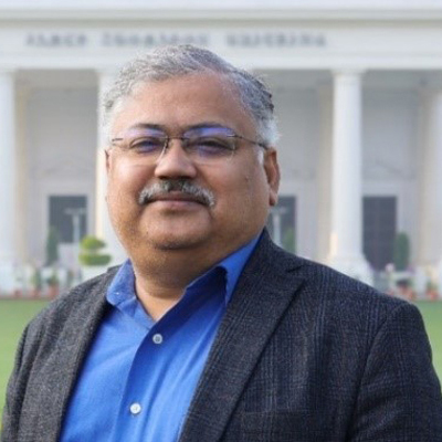
SPEAKERS

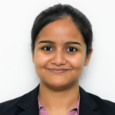
Presenter 1 Image
Venkata Reddy Kolagatla - C-DAC, Bangalore

Venkata Reddy Kolagatla, a Scientist-D at C-DAC Bangalore, has six years of experience in cryptography, ASIC, and SoC design. He previously worked at Synopsys India and Sandisk India, specializing in SDR/DDR memory designs. A Gold Medalist in VLSI Systems from NIT Tiruchirappalli, he also holds a B.Tech in Electronics and Communication Engineering. At C-DAC, he led key ASIC projects and is recognized for his expertise in FPGA/ASIC design and cryptography, with numerous publications to his name.

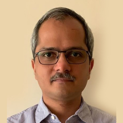
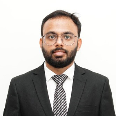
Presenter 2 Image
Shramona Roy - C-DAC, Bangalore

Shramona Roy, a Project Engineer at C-DAC Bangalore for the past two and a half years, holds a B.Tech and M.Tech in Electronics and Communication Engineering from IIITDM Kancheepuram, specializing in VLSI Design. She focuses on low-power Analog and Mixed-Signal circuit designs for wearable electronics and edge IoT. Her research interests include artificial bio-neurons, neuromorphic encoders, and physical security of chips. Shramona leads the Analog/Mixed-Signal design team under the Chips-to-Startup Programme, working on custom front-end ASICs and training initiatives. She has published several papers, including an award-winning one on SAR ADC design.

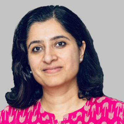
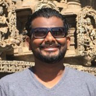
Presenter 3 Image
Vivian Desalphine - C-DAC, Bangalore

Vivian Desalphine is a Scientist-F at C-DAC Bangalore with around 19 years of experience. He is currently involved in the Chips-to-Startup Programme, Design Linked Incentive, and RISC-V GPU development. His work spans several national projects, including microprocessor development, cryptographic module validation, and high-performance network analysis tools. His expertise includes digital VLSI design, RISC-V microprocessor and GPU IP core development, secure microprocessor architectures, and SoC design. He holds a B.Tech in Electronics and Communications from the University of Kerala and a Master's in Digital Signal Processing from the University of Strathclyde, UK. He has numerous publications, a patent, and has contributed to industry technology transfers.

TUTORIAL 2 - Emerging Technologies

Forenoon - Performance-specific, Technology Look-up Table-based Design Methodology for Low-Dropout Voltage Regulators (LDOs)

This tutorial addresses the challenges of using the conventional square-law model to predict MOSFET characteristics in advanced CMOS nanometer technologies and introduces the Technology-Lookup Table (LuT) based design method as a more accurate alternative. This method leverages SPICE-generated LuTs, which include critical MOSFET figures of merit, and are integrated into the circuit design flow to reduce the gap between simulations and hand analysis. However, a single LuT-based approach is insufficient for diverse analog circuits, necessitating customized design algorithms. The tutorial focuses on applying these tailored LuT-based design flows to Low-Dropout Voltage Regulators (LDOs), addressing specific performance requirements like noise rejection, load conditions, and transient response, with examples provided for RF, digital ASIC, and IoT applications in a 180-nm CMOS process.

SPEAKERS

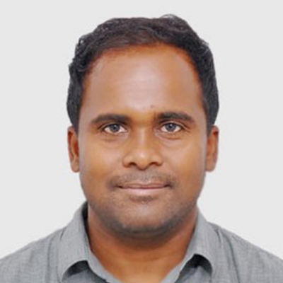
Presenter 2 Image
Sakshi Arora - IIIT Bangalore

Sakshi Arora completed her Ph.D. in Electrical Engineering, specializing in Power Management IC design, at Stanford University in 2013. Prior to her doctoral studies, she worked as an Analog IC Designer at ST Microelectronics from 2005 to 2007. Her doctoral thesis focused on high-frequency multiple output DC-DC converters for SoC (System-On-Chip) applications. She holds a Bachelor of Engineering degree from BITS, Pilani. Following her Ph.D., she worked at Texas Instruments' Kilby Labs in 2014. Subsequently, she served as a Hardware Engineer and Tech Lead at Apple from 2014 to 2019. She is presently working as an Assistant professor at International Institute of Information Technology Bangalore (IIITB), India.

Presenter 1 Image
Manikandan R R - NIT Tiruchirappalli

Manikandan R R received his Ph.D. degree from Electrical Communication Engineering, Indian Institute of Science, Bangalore in 2014. His Ph.D. thesis focused on "Low power and low spur frequency synthesizer circuit techniques for energy efficient wireless transmitters". From 2015 to 2016, he worked as a Lead Design Engineer at Cadence Design Systems, Bangalore. From 2016 to 2017, he was a member of Kilby Labs, Texas Instruments, Bangalore, and designed ultra-low power analog circuits for IoT power management applications. From 2017 to 2023, he worked as an Analog Design Engineer at Texas Instruments, designing isolated power and data transfer circuits and precision analog circuits. From 2023 to 2024, he worked as an Assistant Professor at International Institute of Information Technology Bangalore (IIITB), India.

Afternoon - A Journey across Cryo-CMOS for Quantum Computation

This tutorial explores the significance of Cryo-CMOS technology in advancing quantum computing by integrating classical and quantum components at cryogenic temperatures. Cryo-CMOS circuits, crucial for controlling and reading out qubits, operate at ultra-low temperatures, enhancing electron mobility, reducing noise, and preserving quantum coherence, which is vital for reliable quantum computations. The technology facilitates seamless communication between quantum processors and classical systems, contributing to the scalability and practicality of large-scale quantum computing. Additionally, the tutorial highlights the challenges in cryogenic systems, including thermal management, material selection, device reliability, and integration with conventional electronics. Despite these challenges, Cryo-CMOS technology holds the promise of revolutionizing computing capabilities, particularly in fields such as cryptography, optimization, and drug discovery, by enabling the mass production of quantum-compatible electronics and the realization of silicon-based quantum computers.

SPEAKERS

Presenter 2 Image
Prof. Sudeb Dasgupta - IIT Roorkee

Sudeb Dasgupta is a Professor in the Microelectronics and VLSI Group at IIT Roorkee, with a Ph.D. in Electronics Engineering from IIT-BHU. He has over 250 research publications and has managed research projects worth around ₹5 crores. His research focuses on AI, machine learning, nanoelectronics, and low-power device design, including FinFETs and TFETs. He has guided 14 Ph.D. scholars and is currently supervising about 10 more. He is a member of several professional organizations, including IEEE and the Institute of Nanotechnology, UK.

Presenter 1 Image
Prof. Navjeet Bagga - IIT Bhubaneswar

Dr. Navjeet Bagga is an Assistant Professor at IIT Bhubaneswar, specializing in semiconductor device modeling, nanoscale devices, cryogenic CMOS, and FET-based sensors. He earned his Ph.D. from IIT Roorkee in 2019 and completed post-doctoral research at Karlsruhe Institute of Technology, Germany. Before joining IIT Bhubaneswar, he taught at IIITDM Jabalpur. With over 90 published papers and three best paper awards, he actively collaborates with national and international researchers. He is a Senior Member of IEEE, a Life Member of IETE, and serves as an editor and reviewer for several scientific journals.

TUTORIAL 3 - VLSI Testing & Testability (With Hands-on Labs)

This course provides a comprehensive overview of advanced Design for Testability (DFT) techniques crucial for enhancing IC performance, efficiency, and reliability, with a focus on achieving higher yields measured in Defective Parts Per Billion (DPPB). It covers fundamental and advanced topics, including fault modeling, SCAN and compression techniques, and Chiplet-level DFT strategies like BSDL. Participants will also explore emerging 3D IC testing concepts and BIST methodologies for RAMs and ROMs. The hands-on lab sessions will guide participants through netlist synthesis, SCAN insertion, ATPG, simulations, and a detailed analysis of ATPG log files and waveforms.

SPEAKERS

Presenter 2 Image
Dr. Renold Sam - Microchip Technology Inc. Canada

Renold Sam earned his Doctorate degree in the field of DFT for FinFET circuits. With 20+ years of experience in DFT, he is currently working as a Sr. Manager DFT in Microchip Technology Inc., Vancouver, Canada. He manages teams across 4 geographical locations including North America and Asia continents, handling a team of 65+ engineers. His skillset includes advanced fault modeling and post-silicon debug. He is passionate about teaching and works as an Adjunct Professor at IIIT Chennai. He loves to travel and explore different islands.

Presenter 1 Image
Yadu Krishnan - Microchip Technology Inc. India

Yadukrishnan Gopinathan is a Digital VLSI specialist holding a Master’s degree in Digital VLSI Design. With 4 years of industry experience in the Design For Testability (DFT) domain, Yadukrishnan possesses expertise in digital ICs, system design, and signal processing. His skillset includes scan insertion, ATPG, simulation, and advanced fault modeling. He previously worked as a Silicon Design Engineer at Advanced Micro Devices (AMD) for 2.5 years and currently works as a Design Engineer specialized in Design for Testability at Microchip Technology Inc.

Presenter 2 Image
Prathiba M - Vellore Institute of Technology, Vellore

Prathiba Muthukrishnan earned her B.E. in Electronics and Communication Engineering in 2018 and M.E. in Applied Electronics in 2020 from the College of Engineering Guindy, Anna University. She is now a Senior Research Fellow in her fourth year at Vellore Institute of Technology, Vellore. Her research focuses on digital VLSI testing, particularly small delay defects. She has also collaborated with industry professionals and research supervisors to establish a DFT lab at VIT within the Department of Micro and Nanoelectronics. Her expertise includes hands-on experience with Siemens DFT tools like TessentScan, TessentFastScan, Testkompress, and MBIST.

TUTORIAL 4 - Design Implementation (RTL to GDSII Flow with Hands-on Labs)

This tutorial covers the physical design flow of converting a RTL design to a ready-to-fabricate GDSII layout using Synopsys tools. Participants will learn along with hands-on labs, about various stages including Synthesis, floorplanning, placement, clock tree synthesis, routing & signoff checks to achieve design closure and ensure manufacturability. Practical exercises and hands-on design will enhance the understanding of the tools and methodologies involved in the physical design process.

SPEAKERS

Presenter 1 Image
Vijay Kanth - VLSIMONKS Design Pvt Ltd

Vijay has over 13+ years of experience in the VLSI industry, specializing in physical design, team leadership, and entrepreneurship. He is the co-founder and CEO of VLSIMONKS Design Pvt Ltd, a VLSI service company based in Bangalore, focusing on physical design, logical design, and verification. He began his career at Soctronics and later worked at AMD (Hyderabad) and Qualcomm (Bangalore) before founding VLSIMONKS. Vijay holds a Bachelor's Degree in Electronics and Communications from LBRCE Engineering College, affiliated with JNTU Kakinada.

Presenter 2 Image
Mohan Ganugapati - VLSIMONKS Design Pvt Ltd

Mohan Ganugapati has over 5+ years of experience in physical design and is a Senior Design Engineer at VLSIMONKS Design Pvt Ltd, a VLSI service company based in Bangalore. His previous experience includes working at Broadcom (Bangalore) and Nanoxplore (France). Mohan completed his Master’s in VLSI & Embedded Systems from LBRCE Engineering College, affiliated with JNTU Kakinada, and his Bachelor’s Degree in Electronics & Communications from NRIIT Engineering College, affiliated with JNTU Kakinada.

Presenter 1 Image
Sreedevi Kulkarni - ChipEdge Technologies Pvt. Ltd

Sreedevi Kulkarni is a Member of Technical Staff at ChipEdge Technologies with 12 years of experience teaching VLSI subjects. Prior to joining ChipEdge, she worked as an Assistant Professor at Angadi Institute of Technology & Management, Belgavi. She holds a B.Tech from UBDT College of Engineering, Davanagere, and an M.Tech from Gogte Institute of Technology, Belgaum.

TUTORIAL 5 - VLSI Design & Reliability

Session 1: Life cycle and development of custom Standard cells

Custom standard cells are tailored components in semiconductor design, optimized for specific performance, power, and area requirements. Engineers design these cells with precise transistor sizes and layouts, ensuring they meet exact specifications. Characterization and validation are crucial, involving extensive testing to produce accurate timing models. Once verified, these cells are integrated into design libraries, allowing for efficient IC development. Continuous optimization keeps the cells aligned with advancing technology and design needs.

SPEAKER

Aquib Quraishi Image
Aquib Quraishi - Marvell Technologies

Aquib Quraishi is a Staff Engineer at Marvell Technologies, specializing in Custom Logic Library Development, with over 8 years in the semiconductor industry. His career includes roles at Arm Embedded Technologies, Marquis Technologies, and Qualcomm, where he worked on standard cells and Snapdragon chipsets. Aquib is dedicated to advancing technology nodes and professional growth. Outside work, he enjoys cricket, cooking, traveling, learning new languages, and music.

Session 2: Impact of Design for Test on the production of a Chip

This session aims to provide an overview of how Design For Test (DFT) is implemented in the industry to achieve minimal yield loss, provide defect free SoCs to the customer. This tutorial covers basic concepts and components of DFT, the DFT implementation strategy and the impact of DFT on design and cost. It will cover two realtime case studies each for pre and post silicon scenarios from Marvell Designs. Speakers

SPEAKERS

Aanand Venkatachalam Image
Aanand Venkatachalam - Marvell Technologies

Aanand is Director of Engineering in the Central CAD and Design Services group at Marvell Technology, Bangalore. A seasoned professional with 20 years of experience in DFT architecture, implementation, and silicon bring-up across complex ASICs. He has proficient knowledge in end-to-end DFT activities including Test Planning, Test Logic insertion, hand-off in different EDA environments. He has solid experience in leading DFT efforts with aggressive design schedules, efficient task allocation, and providing technical leadership. He has built and scaled up high-performance teams from scratch for different organizations, including Broadcom, Capgemini, Intel Mobile Communications, Infineon, and Conexant.


Suraj MC Image
Suraj MC - Marvell Technologies

Suraj MC is Principal Engineer in the Central CAD and Design Services (CCDS) team, part of Central Engineering at Marvell Technology, Bangalore. He has around 14 years of extensive experience in DFT from architecture to silicon bring-up. He graduated in Electronics and Communication from Government Engineering College, Kannur in 2008. His DFT career includes work from architecture to silicon debug on complex SoC designs with companies such as Intel, Broadcom, Analog Devices, and PMC Sierra. Suraj has contributed to various technical conferences through papers on the latest DFT methodologies and practices. He recently conducted a session on "targeting bridges and opens using a physical defect-oriented approach" as an industry session speaker at IEEE ITC 2024, Bangalore, on behalf of Marvell.

TUTORIAL 6 - Internet of Things

LoRaWAN (Long Range Wide Area Network) is a key technology in the Industrial Internet of Things (IIoT), offering long-range communication, low power consumption, and secure data transmission. It supports wireless, battery-operated devices across regional, national, or global networks, making it ideal for remote or expansive industrial applications. LoRaWAN enables real-time monitoring, predictive maintenance, asset tracking, and environmental monitoring with minimal power usage, allowing devices to operate for years on a single battery. Its ability to connect numerous devices and integrate with cloud-based platforms enhances scalability and data analytics in industrial operations.

SPEAKER

Dr. Subramanian Image
Dr. K Subramanian - Enthu Technology Solutions India Pvt Ltd

Dr. K Subramanian has over 13 years of industry experience in Embedded Systems and IoT device applications. He has trained numerous professionals and faculty at various top engineering institutions in India. Currently, he is a Technical Lead at Enthu Technology Solutions India Pvt Ltd, Coimbatore, Tamil Nadu.

TUTORIAL 7 - System Design

This tutorial introduces the state of the art techniques to enhance the performance of the digital system for digital signal processing (DSP) and also introduces the role of approximate hardware design concepts in the digital signal processing and image/ video processing applications. In the ever-evolving landscape of DSP, the demand for robust and efficient image and video watermarking systems has grown exponentially. This tutorial session delves into the design and implementation of energy-efficient Very-Large-Scale Integration (VLSI) architectures for DSP, focusing specifically on image and video watermarking systems deployed on Field-Programmable Gate Arrays (FPGAs). The session explores various VLSI design methodologies that optimize power consumption without compromising performance. Through detailed case studies and practical examples, the tutorial will illustrate the effectiveness of proposed architectures in real-world scenarios. This session is ideal for researchers, engineers, and practitioners who are keen on enhancing their knowledge of energy-efficient DSP systems and advancing the state-of-the-art in image and video watermarking technology.

SPEAKERS

Dr. Noor Mohammed Image
Dr. Noor Mohammed - Indian Institute of Information Technology, Design and Manufacturing, Kancheepuram

Dr. Noor Mohammed received his Ph.D. in Computer Science and Engineering from Indian Institute of Technology Madras, Chennai, in 2009. He completed his M.Tech. in Electronics Design Technology from the Centre for Electronics Design and Technology of India (CEDTI) (now known as National Institute of Electronics and Information Technology Aurangabad), Aurangabad, in 2003, and B.Tech. in Electronics and Communication Engineering from NBKR Institute of Science and Technology, Vidyanagar, Sri Venkateswara University, Tirupati, in 2001. He has published many papers in international journals and conferences.

Dr. Dhayalakumar M Image
Dr. Dhayalakumar M - Dissai Technologies

Dr Dhayalakumar M, Founder of Dissai Technologies. He has received his M. Tech., and PhD from IIITDM Kancheepuram.

TUTORIAL 8 - Design Verification

This tutorial focuses on the increasing demand for specialized processors in fields like automotive, medical, defense, and aeronautics, necessitating architectural advancements and new packaging technologies like 2.5D/3D and Chiplets. While traditional ISAs like X86 and ARM require expensive royalties, the open-source RISC-V ISA offers flexibility for designing specialized processors and software development. The tutorial will discuss the benefits of RISC-V and the importance of mastering functional verification for First-Pass Silicon success, especially for RISC-V-based processors and SoCs. It highlights that despite advancements in AI-driven EDA tools, functional verification remains critical, with over 70% of ASICs requiring multiple re-spins due to logic and functional flaws. The tutorial will cover verification techniques such as simulation, formal methods, hardware acceleration, and prototyping, along with methodologies like Constrained Random Coverage Driven Verification (CRCDV) and Portable Test Stimulus Standard (PSS), demonstrated through a RISC-V design verification demo.

SPEAKER

Putta Satish Image
Putta Satish - Principal Engineer, Maven Silicon

Putta Satish holds an experience of 14+ years in the field of VLSI Verification and Training. He has worked as a verification engineer for various companies like IBM on the development of TB for DDR Memory controllers resulting in successful tape out of the chip that was used in IBM’s server Z. And also, he worked at Aceic Design Technologies on the development of VIP for Bluetooth Low Energy. As a trainer at Maven Silicon, he successfully delivered various trainings for new college graduates and corporate trainings on SystemVerilog and UVM at various companies that include the World’s Largest WiFi MNC Technology Company, World’s Largest Mobility Solutions Provider, Leading IP/EDA tool provider company to name a few. He now specializes in offering training services on RISC-V and ARM architectures and he was trained by ARM on ARM V8A Architecture as Maven Silicon is an ARM Approved Training Partner (AATP). He is the recipient of the "Outstanding Technical Contribution" award from Aceic Design Systems and holds a Master’s degree in VLSI Design from VIT University, Vellore.

TUTORIAL 9 - Physical Verification

Session 1: Challenges and Solutions during Low Power Mixed Signal (LPMS) SoC Verification

This tutorial addresses the challenges and solutions in Mixed Signal verification, emphasizing the need to enhance verification efficiency by reducing simulation and debug cycle times. It explores various issues encountered during LPMS (Low Power Mixed Signal) verification, including problems with domain conversion elements, user errors, low power boundary handling, modeling mistakes, simulation performance, and IP integration. Through real-world examples, the tutorial provides insights into overcoming these challenges, offering techniques to help verification engineers and architects speed up the identification and resolution of critical design issues, ultimately improving time-to-market.

SPEAKER

Lalit Mohan Image
Lalit Mohan - Cadence Design Systems India

Lalit Mohan has 18+ years of experience in Analog and Mixed Signal Modeling and Verification. He is working with Cadence Global Customer support team as AMS Application Engineer. Lalit has authored 350+ technical articles including Application Notes, Rapid Adoption Kits Videos, etc., on Analog and Mixed Signal domain. He is the author of the famous application note “Seven Habits of Highly Efficient Mixed Signal Verification Engineers” available at Cadence Online Support. Lalit has published multiple papers and posters in technical Industrial Conferences. Lalit owns a LinkedIn group on Analog Mixed Signal Verification where he posts AMS technologies regularly. Lalit has a Master’s degree in VLSI design from CDAC Noida and a Bachelor’s degree from AMIETE Delhi. His interest areas include AMS, SV RNM modeling and verification.

Session 2: Design Rules: Concepts, Checking, DRC Aware Place & Route for Custom Flow

The rapid and exponential growth in the electronics industry has been driven by the ability of semiconductor manufacturers to rapidly shrink the processes. This has allowed integrated circuits to pack in progressively larger functionality in smaller areas, with higher performance at a lower per-transistor cost. The resolution limit of traditional optical lithography was overcome with the use of various resolution enhancement techniques (RETs). This tutorial talks about the constraints imposed by RETs and how these constraints translate into specific design rules. This includes an analysis of design restrictions and the modeling of these restrictions into rules such as Optical Proximity Correction (OPC), Phase-Shift Masks (PSM), Litho-Etch-Litho-Etch (LELE), and Self-Aligned Dual Patterning (SADP). The tutorial further explores the modeling of design rules through both sign-off and in-design checking, emphasizing geometric operations and constraint-based methodologies. The tutorial will further cover constraint scoping, covering various aspects including foundry, design, net, and region constraints. The discussion extends to the implementation of design rules-aware custom design flow, focusing on rule checking in both interactive and batch modes, as well as rule-aware editing and place-and-route processes. Finally, the tutorial addresses the strategies for rule fixing, distinguishing between automated and assisted fixing approaches. This tutorial aims to provide a thorough understanding of the design rules that underpin the VLSI design flow, ensuring robust, reliable, and manufacturable integrated circuits using DRC Checking Tool provided by Cadence Virtuoso.

SPEAKERS

Sachin Shrivastava Image
Sachin Shrivastava

Sachin has 21 years of industry experience and is currently working as Software Engineering Director at Cadence. He received his M. Tech. in Communications Technology from IIT Kanpur. He holds 13 US patents and has published 12 technical papers at various international conferences.

Vishal Rastogi Image
Vishal Rastogi

Vishal has 21 years of IT industry experience and is currently working with Cadence as Senior Principal Software Engineer. He did his B.Tech. in Computer Science from MNNIT, Allahabad, and an MBA from IIM Lucknow. He is currently focusing on new tech node challenges related to design rules and leading efforts to enable new tech nodes within Virtuoso®. He has filed patents on advanced cut-metal insertion and has published papers on layout methodologies.

Deepak Karnatak Image
Deepak Karnatak

Deepak has 16 years of industry experience across EDA, telecom, and network security. He is an engineering graduate from MNNIT, Allahabad, and is currently working with Cadence as Senior Principal Software Engineer. His current focus is on finding solutions for advanced placement and routing techniques. He has filed a patent on advanced cut-metal insertion and has published a paper on layout methodologies.