- Centre for Functional Materials(CFM)-Events-International Workshop
- Home
- Centre for Functional Materials(CFM)-Events-International Workshop
Centre for Functional Materials(CFM)-Events-International Workshop
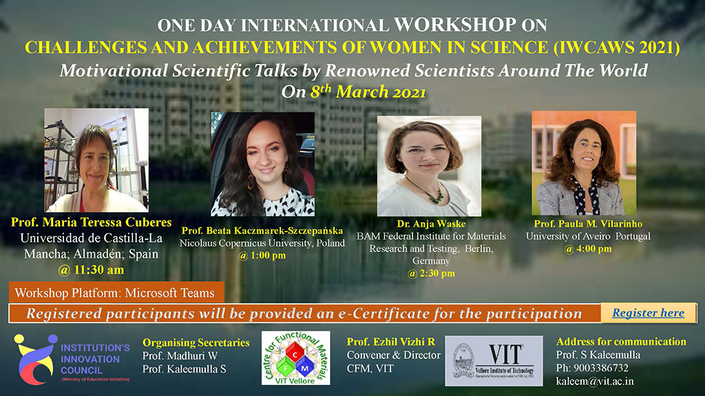
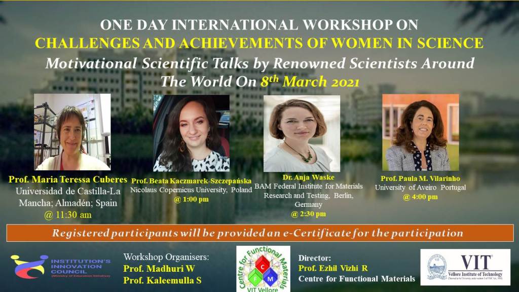
One Day International Workshop on Challenges and Achievements of Women in Science
Motivational Scientific Talks by Renowned Scientists Around The World On 8thMarch 2021
Session 1 (@ 11:30 am)
Title: Learning About Materials on the Nanoscale with Scanning Probe Microscopes
Prof. Maria Teressa Cuberes
Universidad de Castilla-La Mancha; Almadén; Spain
Read Abstract
Scanning Probe Microscopy (SPM) provide invaluable tools for the characterization and manipulation of materials on the nanoscale. In this Seminar I will introduce the basics of these techniques and illustrate some SPM-based procedures which I have contributed myself to develop along my scientific career. In particular, I will discuss the technique of Ballistic Electron Emission Microscopy (BEEM), and its possibilities for the characterization of the electronic response at semiconductor interfaces [1], and other possible applications. In addition, I will share several examples of the use of Scanning Probe Microscopy for the manipulation of individual molecules, and how to learn about materials self-assembling from this kind of experiments. [2] Eventually, I will introduce a the techniques of Atomic Force Microscopy with ultrasound excitation, and their application to study of nanoscale dynamic elastic, viscoelastic and adhesive properties on both hard and soft samples, and to provide subsurface information[3].
About the Speaker
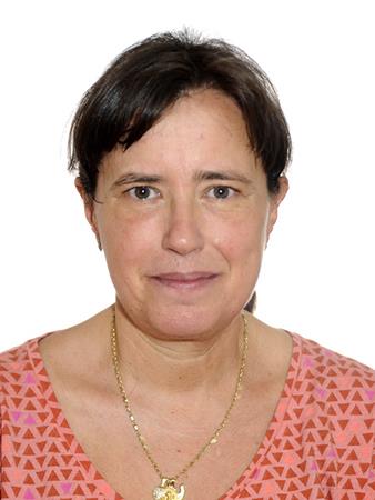 Prof. Maria Teressa Cuberes
Degree in Physics (Materials Science) in 1987, and Ph.D. in Physics in 1991, in the University Complutense of Madrid, in Spain. Graduate student in the Materials Science Institute in Madrid (Consejo Superior de Investigaciones Científicas, CSIC) from 1987-1991. Postdoc in the Institute of Experimental Physics, in Berlin (Germany) from 1992-1993, in the Institute of Materials Science in Madrid (CSIC) from 1994-1995 and in IBM Zurich (Switzerland) from 1996-1997. Research assistant in the Department of Materials, University of Oxford (UK) from 1997-1998. Assistance Professor in the Engineering School of Almaden, University of Castilla-La Mancha (UCLM) from 1998-2000 Lecture in the Engineering School of Almaden (UCLM) from 2000-2003. Professor in Materials Science and Engineering in the Engineering School of Almaden (UCLM) from 2003 up to date. Research experience in Scanning Probe Microscopy techniques, semiconductor interfaces, thin polymer films and molecular layers, Ultra-High Vacuum, Synchrotron Radiation, Surface Spectroscopies, nanoscale electrical and mechanical properties.
- 1. Cuberes, M.T.; Bauer, A.; Wen, H.J.; Prietsch, M.; Kaindl, G. Ballistic Electron Emission Microscopy Study of the Au/Si(111)7X7 and Au/CaF2/Si(111)7X7 interfaces. Applied Physics Letters 1994, 64, 2300-2302, doi:10.1063/1.111650.
- 2. Cuberes, M.T.; Schlittler, R.R.; Gimzewski, J.K. Room-temperature repositioning of individual C60 molecules at Cu steps: Operation of a molecular counting device. Applied Physics Letters 1996, 69, 3016-3018, doi:10.1063/1.116824.
- 3. Marino, S.; Joshi, G.M.; Lusuardi, A.; Cuberes, M.T. Ultrasonic force microscopy on poly(vinyl alcohol)/SrTiO3 nano-perovskites hybrid films. Ultramicroscopy 2014, 142, doi:10.1016/j.ultramic.2014.03.012.
Session 2 (@ 1:00 pm)
Title: Nanotechnology in cosmetics - opportunities or challenges?
Prof. Beata Kaczmarek-Szczepańska
Nicolaus Copernicus University, Poland
Read Abstract
Nanotechnology found application in cosmetics. They provide many advantages as high activity, transparency, solubility, etc. However, there are many concerns about the safety of such nanocosmetics. During the lecture, I will discuss the regulations of nanoparticles used in the cosmetic industry, as well as the opportunities and challenges of their application in cosmetics.
About the Speaker
Dr. Beata K Szczepanska
Working as assistant professor in the department of Biomaterials and cosmetic chemistry at Nicolaus Copernicus University, Poland. Dr. Beata is a very active researcher and has completed 5 funded research projects and a project is in force funded by the Poland National Science Centre. Dr. Beata has published more than 55 research articles and 3 book chapters.
She is Editorial Board Member of Current Cosmetic Science journal (Bentham Science); Guest Editor in Special Issue "Biopolymers: Synthesis, Properties and Biological Applications" (Materials journal, Guest Editor in Special Issue "Thin Films for Biomedical Application"
Session 3 (@ 2:30 pm)
Title: X-ray Non-destructive testing of materials and composites
Dr. Anja Waske
BAM Federal Institute for Materials Research and Testing, Berlin, Germany
Read Abstract
Using magnetic materials for energy conversion as an example, this lecture shows how X-ray tomography investigations can contribute to structure elucidation in composites and solid samples. The components are tested non-destructively in order to characterize cracks, pores and other defects and their influence on the functional properties three-dimensionally and in good time in the life cycle of the material. If one combines microtomography with other methods of magnetic material characterization, unique statements about the structure and the functional properties are possible.
About the Speaker
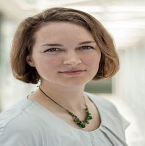 Dr.-Ing. Anja Waske
Head of division "Radiological Methods" at the Federal Institute for Materials Research and Testing (Bundesanstalt für Materialforschung und -prüfung, BAM), Berlin. She studied physics at the Technische Universität Dresden, Germany, followed by a PhD degree in the field of X-ray tomographic characterization of granular matter. Her research field is at the interface of materials science and X-ray imaging. Her group develops 3D X-ray imaging methods and analysis routes for 3D image data for understanding the properties of functional, structural and additively manufactured materials.
Session 4 (@ 4:00 pm)
Title: Spark Plasma Texturing: a technology development for lead free pioezoelectrics
Prof.Paula M. Vilarinho
University of AveiroPortugal
Read Abstract
This talk addresses the sintering of undoped lead free piezoelectric (K1-xNax)NbO3 (KNN) ceramics by Spark Plasma Texturing (SPT) and compares their properties with equivalent ceramics prepared by Spark Plasma Sintering (SPS). I will describe the interplay between materials structure, microstructure, electrical conductivity, and non-linear dielectric properties for SPT KNN and the implications of these relations for enhancing electrical properties. Functional oxides, which include piezoelectric ceramics, are used in a wide variety of applications, from industrial machinery to compact electronic equipment and tools. Moreover, the Internet of Things is becoming a commodity, thus increasing the need for sensors and actuators. Consequently, it is expected that the overall market for piezoelectric devices will reach $31.33 billion by 2022. KNN is one of the most promising lead-free piezoelectric system to replace lead based piezoelectrics, mainly due to its high Curie temperature. Dense KNN ceramics require relatively high sintering temperatures, not compatible with the high vapour pressure of alkaline elements and thus alternative processing techniques are required. In this work we exploited the use of one derivative method of SPS that is Spark Plasma Texturing (SPT) defined as an edge-free SPS. We conclude that d33 (108 pC N-1), g33 (21.2×10⁻³ Vm N-1), Pr (19.7 μC cm-²) and Ec (11.9 kV cm-1) are significantly improved in undoped KNN ceramics processed, SPT. SPT KNN ceramics have a more homogeneous electrical microstructure with small grain size and narrow grain size distribution. SPT, as with hot-forging, results in neck destruction, particle rearrangement, and destruction of agglomerates improving the density and limiting grain coarsening, affecting point defects creation / distribution, giving rise to a rather homogeneous defect distribution. Consequently, SPT KNN ceramics grain cores and shells have similar resistance and capacitance behaviours. We hypothesise that, the electrical homogeneity of SPT KNN ceramics may along with the smaller grain size and higher density increase electric breakdown strength (EBDS) (of high relevance for industrial applications). In addition, the resultant compressively stressed lattice enhances the dielectric and piezoelectric performance.
About the Speaker
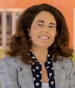 Prof.Paula M. Vilarinho
Vilarinho is Associate Professor at University of Aveiro (UA) since 2000 and a Senior Researcher of Associate Laboratory, CICECO – Aveiro Materials Institute. Currently she is: i) leader of the Electroceramics Group, within CICECO, ii) President of the Portuguese Society of Materials (SPM), iii) Coordinator (Portugal) of the Emerging Technologies Program within The University of Texas at Austin – Foundation for Science and Technology (FCT) Portugal Program, iv) Member of the Scientific Committee of the Doctoral Program in Materials Science and Engineering, UA. She was Visiting Professor at Dep of Materials Science and Engineering of North Carolina State University, USA, 2001, Visiting Professor at Dep of Materials Science and Engineering, University of Sheffield, United Kingdom, 2008 and Visiting Professor at McKetta Dep of Chemical Engineering, University of Texas at Austin, Texas, USA, 2015. She was: i) Director of Undergraduate Course in Ceramics and Glass Engineering, UA (1999-2001), and Director of Undergraduate Course in Materials Engineering, UA (2009-2016), ii) coordinator of Scientific Commission of Dep of Ceramics and Glass Engineering, UA (2002-2006), iii) former President of Portuguese Society of Microscopy (2010 - 2011), iv) former vice-president of Portuguese Materials Society (SPM) (2009-2013). She is: i) member of the Editorial Board of Scientific Reports (Nature Publishing Group), Processing and Application of Ceramics and International Scholarly Research Network - ISRN Ceramics, ii) member of Portuguese, European and American Materials Research Societies and Microscopy Societies, iii) referee in the selection of Portuguese and European R&D projects and National Science Foundation (NSF) USA, as well as a frequent referee of SCI journals. Vilarinho published over 295 papers, 6 book chapters, with ca. 5424 citations (h-index 38), 10 patent applications and edited 4 books. She has given over one hundred scientific and technical talks at international conferences and 135invited talks. She has(is) supervised(ing) 20 post-docs, 25 PhD students and 46 Master students. She has been involved and coordinating more than 20 R&D projects and in more than 20 European R&D actions, networks and projects on the development and characterization of dielectric, piezoelectric and ferroelectric materials. She organized 8 and co-organised 6 International Scientific Meetings and more than 12 National and International workshops on Materials Science topics. She was distinguished with the prize “Estímulo à Excelência” (Stimulus to Excellence) in February 2007 awarded by the Portuguese Foundation for Science and Technology (FCT). Her profile and scientific career were recently distinguish in the recent book “Successful Women Ceramic and Glass Scientists and Engineers: 100 Inspirational Profiles” by Lynnette Madsen, Willey, 2016. Vilarinho Research Group is engaged in fundamental and applied research in the synthesis, properties and processing of functional materials for electronics, microelectronics and related applications; mainly focused on electrical polarization phenomena in solids, aiming to understand mechanisms that control electrical polarization at the macroscopic and nanoscale level, and applying such understanding to the development of advanced nano and microelectronic devices. Her group has been using electrical and structural characterization tools (impedance spectroscopy, piezo- ferroelectric analysis, scanning probe microscopy, electron microscopy, Raman spectroscopy, etc) at the highest level. Materials under investigation include perovskite type ferroelectric, piezoelectric, dielectric and multiferroic oxides and piezoelectric polymers (PLLA, PVDF). Applications include microelectronic devices as memories, sensor and actuators, energy harvesters, thermoelectric devices, tunable dielectrics, but also and more recently biorelated uses, as bio-compatible piezoelectric platforms for tissue growth, biosensors, etc. The synthesis of nanofunctional materials in different geometries (1D, 2D, 3D) at low temperatures for compatible materials integration and using low cost approaches is becoming increasingly important in her´s research . Vilarinho´s group has been exploiting hydrothermal synthesis, diphasic sol precursors, photo chemical solution and electrophoretic deposition (EPD) for preparation of nanoparticulates, nanocomposites, thin, thick films of functional materials. More recently initiated exploitation of low-temperature budget processes, as FLASH sintering, and Cold Sintering. One of the newest R&D interests of Vilarinho group is related with Additive Manufacturing of ceramic and composite materials. The aim is on one side to explore techniques as 3D Printing and Robocasting for the fabrication of ceramic materials in direct collaboration with Portuguese Ceramic companies, on the other hand to explore Additive Manufacturing of functional ceramics and composite materials for microelectronics.
Interested are requested to register through the link given below.
The registered attendees will be provided an e-certificate for participation in the workshop.
Information related to Recent news, Centre events and Latest announcements related to CFM at VIT Vellore are available here.
