Centre for Functional Materials(CFM)
All Events
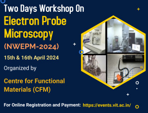
Two days Workshop on Electron Probe Microscopy (NWEPM-2024)
Two days Workshop on Electron Probe Microscopy(NWEPM-2024)
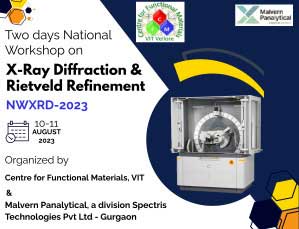
Two days National Workshop on X-Ray Diffraction & Rietveld Refinement (NWXRD-2023)
Two days National Workshop on X-Ray Diffraction & Rietveld Refinement (NWXRD-2023)
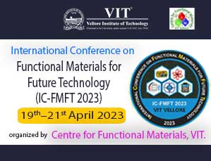
International Conference on Functional Materials for Future Technologies 2023(ICFMFT-2023)
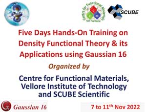
Five Days Hands On Training on Density Functional Theory and its Applications using Gaussian 16
National Workshop
Five Days Hands On Training on Density Functional Theory and its Applications using Gaussian 16
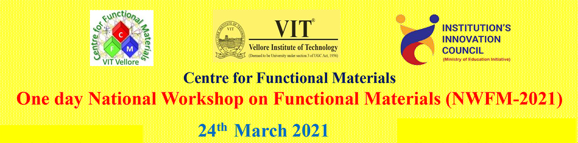
One day National Workshop on Functional Materials (NWFM-2021)

Venue
Schedule
Session 1 (10:00 AM -11:30 AM)
Title: Functional Materials for Defence Application
Dr. Anuj Shukla
Scientist E, Defense Laboratory, Jodhpur, Rajasthan, India.
Venue
Read Abstract
About the Speaker
Session 2 (11:30 AM - 01:00 PM)
Title: Research in DMRL on Nano-materials: Piezoelectrics & Ferroelectrics
Dr. A R James
Scientist F, DMRL, DRDO,Hyderabad, India
Venue
Read Abstract
About the Speaker
Session 3 (02:00 PM - 03:30 PM)
Title: Racetrack Memory Devices: Trapping and Injecting Single Domain Walls in Magnetic Wire
Dr. G. A. Basheed
Senior Scientist, National Physical Laboratory (NPL), New Dehli, India
Venue
Read Abstract
About the Speaker
Session 4 (3:30 PM - 05:00 PM )
Title: Heterojunction Functional Materials for Photoelectrocatalytic Water Splitting
Dr. A. Pandikumar
Scientist, Central Electrochemical Research Institute, Karaikudi, T.N., India.
Venue
Read Abstract
About the Speaker
Interested are requested to register through the link given below.
International Workshop
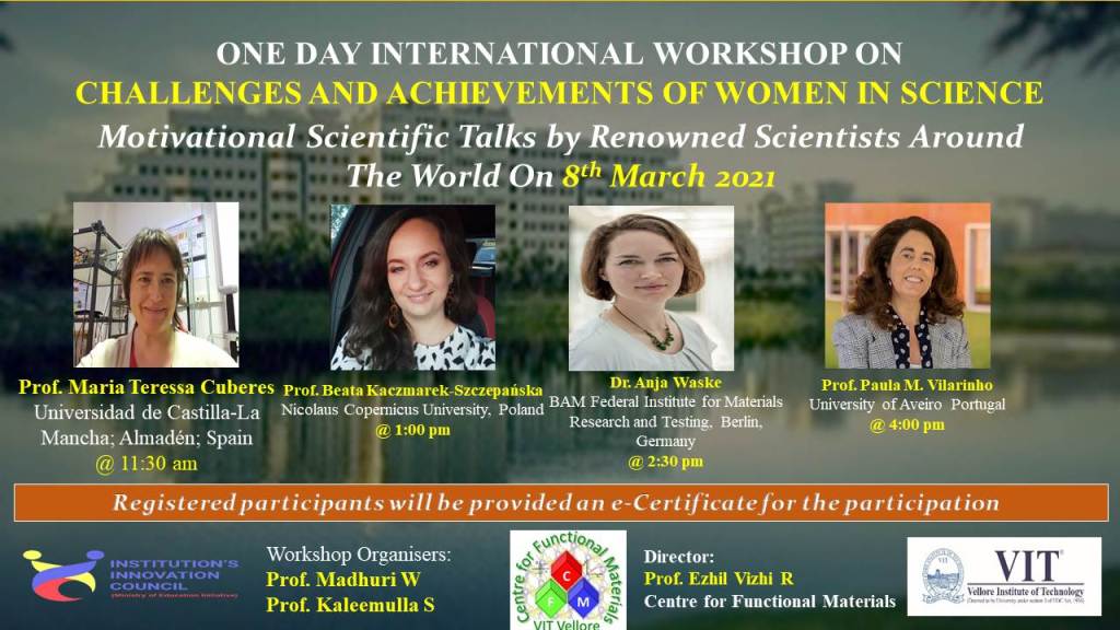
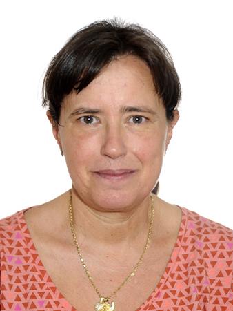
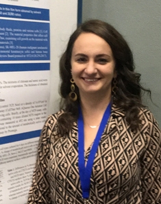
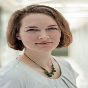
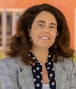
One Day International Workshop on Challenges and Achievements of Women in Science
Motivational Scientific Talks by Renowned Scientists Around The World On 8thMarch 2021
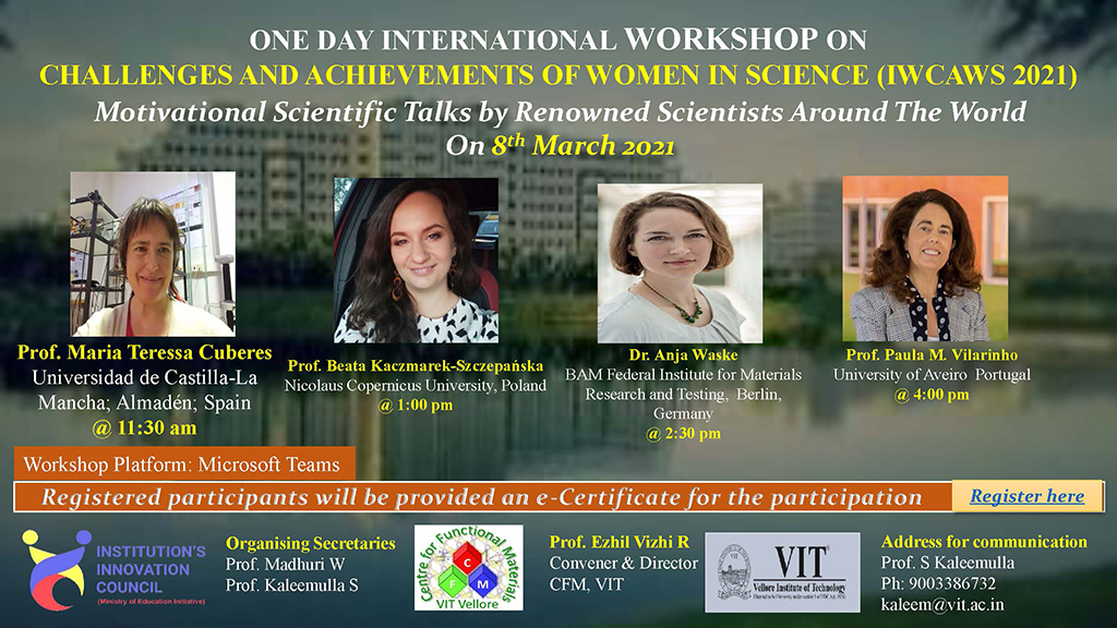
Session 1 (@ 11:30 am)
Title: Learning About Materials on the Nanoscale with Scanning Probe Microscopes
Prof. Maria Teressa Cuberes
Universidad de Castilla-La Mancha; Almadén; Spain
Venue
Read Abstract
About the Speaker
 Prof. Maria Teressa Cuberes
Degree in Physics (Materials Science) in 1987, and Ph.D. in Physics in 1991, in the University Complutense of Madrid, in Spain. Graduate student in the Materials Science Institute in Madrid (Consejo Superior de Investigaciones Científicas, CSIC) from 1987-1991. Postdoc in the Institute of Experimental Physics, in Berlin (Germany) from 1992-1993, in the Institute of Materials Science in Madrid (CSIC) from 1994-1995 and in IBM Zurich (Switzerland) from 1996-1997. Research assistant in the Department of Materials, University of Oxford (UK) from 1997-1998. Assistance Professor in the Engineering School of Almaden, University of Castilla-La Mancha (UCLM) from 1998-2000 Lecture in the Engineering School of Almaden (UCLM) from 2000-2003. Professor in Materials Science and Engineering in the Engineering School of Almaden (UCLM) from 2003 up to date. Research experience in Scanning Probe Microscopy techniques, semiconductor interfaces, thin polymer films and molecular layers, Ultra-High Vacuum, Synchrotron Radiation, Surface Spectroscopies, nanoscale electrical and mechanical properties.
- 1. Cuberes, M.T.; Bauer, A.; Wen, H.J.; Prietsch, M.; Kaindl, G. Ballistic Electron Emission Microscopy Study of the Au/Si(111)7X7 and Au/CaF2/Si(111)7X7 interfaces. Applied Physics Letters 1994, 64, 2300-2302, doi:10.1063/1.111650.
- 2. Cuberes, M.T.; Schlittler, R.R.; Gimzewski, J.K. Room-temperature repositioning of individual C60 molecules at Cu steps: Operation of a molecular counting device. Applied Physics Letters 1996, 69, 3016-3018, doi:10.1063/1.116824.
- 3. Marino, S.; Joshi, G.M.; Lusuardi, A.; Cuberes, M.T. Ultrasonic force microscopy on poly(vinyl alcohol)/SrTiO3 nano-perovskites hybrid films. Ultramicroscopy 2014, 142, doi:10.1016/j.ultramic.2014.03.012.
Session 2 (@ 1:00 pm)
Title: Nanotechnology in cosmetics - opportunities or challenges?
Prof. Beata Kaczmarek-Szczepańska
Nicolaus Copernicus University, Poland
Venue
Read Abstract
About the Speaker
 Dr. Beata K Szczepanska
Working as assistant professor in the department of Biomaterials and cosmetic chemistry at Nicolaus Copernicus University, Poland. Dr. Beata is a very active researcher and has completed 5 funded research projects and a project is in force funded by the Poland National Science Centre. Dr. Beata has published more than 55 research articles and 3 book chapters.
She is Editorial Board Member of Current Cosmetic Science journal (Bentham Science); Guest Editor in Special Issue "Biopolymers: Synthesis, Properties and Biological Applications" (Materials journal, Guest Editor in Special Issue "Thin Films for Biomedical Application"
Session 3 (@ 2:30 pm)
Title: X-ray Non-destructive testing of materials and composites
Dr. Anja Waske
BAM Federal Institute for Materials Research and Testing, Berlin, Germany
Venue
Read Abstract
About the Speaker
 Dr.-Ing. Anja Waske
Head of division "Radiological Methods" at the Federal Institute for Materials Research and Testing (Bundesanstalt für Materialforschung und -prüfung, BAM), Berlin. She studied physics at the Technische Universität Dresden, Germany, followed by a PhD degree in the field of X-ray tomographic characterization of granular matter. Her research field is at the interface of materials science and X-ray imaging. Her group develops 3D X-ray imaging methods and analysis routes for 3D image data for understanding the properties of functional, structural and additively manufactured materials.
Session 4 (@ 4:00 pm)
Title: Spark Plasma Texturing: a technology development for lead free pioezoelectrics
Prof.Paula M. Vilarinho
University of AveiroPortugal
Venue
Read Abstract
About the Speaker
 Prof.Paula M. Vilarinho
Vilarinho is Associate Professor at University of Aveiro (UA) since 2000 and a Senior Researcher of Associate Laboratory, CICECO – Aveiro Materials Institute. Currently she is: i) leader of the Electroceramics Group, within CICECO, ii) President of the Portuguese Society of Materials (SPM), iii) Coordinator (Portugal) of the Emerging Technologies Program within The University of Texas at Austin – Foundation for Science and Technology (FCT) Portugal Program, iv) Member of the Scientific Committee of the Doctoral Program in Materials Science and Engineering, UA. She was Visiting Professor at Dep of Materials Science and Engineering of North Carolina State University, USA, 2001, Visiting Professor at Dep of Materials Science and Engineering, University of Sheffield, United Kingdom, 2008 and Visiting Professor at McKetta Dep of Chemical Engineering, University of Texas at Austin, Texas, USA, 2015. She was: i) Director of Undergraduate Course in Ceramics and Glass Engineering, UA (1999-2001), and Director of Undergraduate Course in Materials Engineering, UA (2009-2016), ii) coordinator of Scientific Commission of Dep of Ceramics and Glass Engineering, UA (2002-2006), iii) former President of Portuguese Society of Microscopy (2010 - 2011), iv) former vice-president of Portuguese Materials Society (SPM) (2009-2013). She is: i) member of the Editorial Board of Scientific Reports (Nature Publishing Group), Processing and Application of Ceramics and International Scholarly Research Network - ISRN Ceramics, ii) member of Portuguese, European and American Materials Research Societies and Microscopy Societies, iii) referee in the selection of Portuguese and European R&D projects and National Science Foundation (NSF) USA, as well as a frequent referee of SCI journals. Vilarinho published over 295 papers, 6 book chapters, with ca. 5424 citations (h-index 38), 10 patent applications and edited 4 books. She has given over one hundred scientific and technical talks at international conferences and 135invited talks. She has(is) supervised(ing) 20 post-docs, 25 PhD students and 46 Master students. She has been involved and coordinating more than 20 R&D projects and in more than 20 European R&D actions, networks and projects on the development and characterization of dielectric, piezoelectric and ferroelectric materials. She organized 8 and co-organised 6 International Scientific Meetings and more than 12 National and International workshops on Materials Science topics. She was distinguished with the prize “Estímulo à Excelência” (Stimulus to Excellence) in February 2007 awarded by the Portuguese Foundation for Science and Technology (FCT). Her profile and scientific career were recently distinguish in the recent book “Successful Women Ceramic and Glass Scientists and Engineers: 100 Inspirational Profiles” by Lynnette Madsen, Willey, 2016. Vilarinho Research Group is engaged in fundamental and applied research in the synthesis, properties and processing of functional materials for electronics, microelectronics and related applications; mainly focused on electrical polarization phenomena in solids, aiming to understand mechanisms that control electrical polarization at the macroscopic and nanoscale level, and applying such understanding to the development of advanced nano and microelectronic devices. Her group has been using electrical and structural characterization tools (impedance spectroscopy, piezo- ferroelectric analysis, scanning probe microscopy, electron microscopy, Raman spectroscopy, etc) at the highest level. Materials under investigation include perovskite type ferroelectric, piezoelectric, dielectric and multiferroic oxides and piezoelectric polymers (PLLA, PVDF). Applications include microelectronic devices as memories, sensor and actuators, energy harvesters, thermoelectric devices, tunable dielectrics, but also and more recently biorelated uses, as bio-compatible piezoelectric platforms for tissue growth, biosensors, etc. The synthesis of nanofunctional materials in different geometries (1D, 2D, 3D) at low temperatures for compatible materials integration and using low cost approaches is becoming increasingly important in her´s research . Vilarinho´s group has been exploiting hydrothermal synthesis, diphasic sol precursors, photo chemical solution and electrophoretic deposition (EPD) for preparation of nanoparticulates, nanocomposites, thin, thick films of functional materials. More recently initiated exploitation of low-temperature budget processes, as FLASH sintering, and Cold Sintering. One of the newest R&D interests of Vilarinho group is related with Additive Manufacturing of ceramic and composite materials. The aim is on one side to explore techniques as 3D Printing and Robocasting for the fabrication of ceramic materials in direct collaboration with Portuguese Ceramic companies, on the other hand to explore Additive Manufacturing of functional ceramics and composite materials for microelectronics.
Interested are requested to register through the link given below.
The registered attendees will be provided an e-certificate for participation in the workshop.