


ASIC Design Lab
ASIC Design Lab
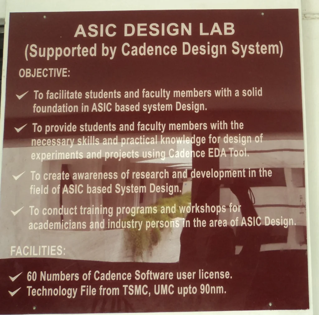
The primary objective of this laboratory course is to understand and implement the complete ASIC Design Flow, navigating the critical path from concept to silicon layout. The workflow is broadly split into Frontend and Backend design. The Frontend phase focuses on architectural logic, beginning with Hardware Description Language (HDL) coding and functional simulation, followed by logic synthesis to convert the code into a gate-level netlist. The Backend (Physical Design) phase translates this netlist into a physical geometric layout through floorplanning, placement, Clock Tree Synthesis (CTS), and routing. By executing this sequence, this lab provides practical insights into balancing the core trade-offs of Power, Performance, and Area (PPA) while ensuring the final layout is free of timing violations and ready for physical fabrication.

| Phase | Lab Objectives |
| Frontend Design (Logic) | * To model and simulate digital designs using Hardware Description Languages (HDLs) like Verilog, SystemVerilog, or VHDL. * To verify functional correctness by writing testbenches and analyzing waveforms using simulation tools. |
| Synthesis & Netlist Generation | * To perform logic synthesis to translate high-level behavioral HDL descriptions into a gate-level netlist using a target standard cell library. * To analyze initial pre-layout timing, area, and power reports to check for structural constraints. |
| Backend Design (Physical) | * To establish the physical chip boundary, aspect ratio, and core rows during the floorplanning phase. * To design a robust power distribution network (Power Planning) to minimize voltage drop (IR drop). * To execute automated standard cell placement to optimize total wirelength and timing density. * To perform Clock Tree Synthesis (CTS) to minimize clock skew and latency across sequential elements. * To run global and detail routing to physically interconnect the signal nets according to the logical netlist. |
| Verification & Sign-off | * To conduct Static Timing Analysis (STA) to ensure setup and hold time requirements are met under various operating conditions. * To run physical verification, including Design Rule Checks (DRC) and Layout Versus Schematic (LVS), to guarantee error-free manufacturing layout generation (GDSII). |