ASIC Design Laboratory
- Home
- Schools
- SENSE
- Facilities
- ASIC Design Laboratory
ASIC Design Laboratory (TT 237A)
Overview
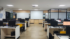
The TT 237A ASIC Design Laboratory is a specialised facility supporting teaching and research in VLSI and ASIC design methodologies. It includes EDA tools and software sponsored by the C2S programme and 55 computer systems for design, simulation, and verification activities.
The laboratory provides access to Cadence, Synopsys, Quartus Prime, and Xilinx Vivado. These industry-standard platforms support design flows from RTL coding and functional simulation to synthesis, verification, and physical design implementation, providing exposure to semiconductor-industry practices.
The laboratory supports undergraduate coursework and projects, postgraduate design experiments, and PhD research in ASIC design, FPGA prototyping, and hardware-software co-design. Its research activities have contributed to publications in journals and conferences as well as patents.
Objectives
- Provide robust computing infrastructure for VLSI and ASIC design tasks.
- Offer hands-on training with industry-standard EDA tools.
- Support academic and research activities at UG, PG, and PhD levels.
- Promote innovation through publications, patents, and advanced prototyping.
ASIC Design Laboratory
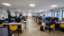
ASIC Design Laboratory – lab session
Key Focus Areas
- VLSI and ASIC design methodologies – design, simulation, and verification.
- EDA tool utilisation – training with Cadence, Synopsys, Quartus Prime, and Xilinx Vivado.
- Academic and research support – UG, PG, and PhD projects and investigations.
- FPGA and hardware-software co-design – prototyping and system integration.
- Innovation and knowledge creation – publications, patents, and research contributions.