


Chip Design Lab
- Home
- Schools
- SENSE
- Facilities
- Chip Design Lab
Chip Design Lab
Overview
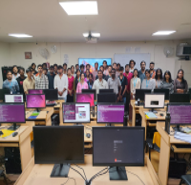
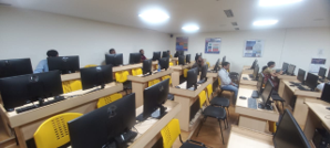
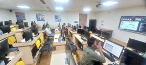
The Chip Design Lab is a core teaching and practical training facility under the School of Electronics Engineering (SENSE), Vellore Institute of Technology (VIT), Vellore, established to provide hands-on experience in digital integrated circuit design, ASIC design methodologies, and VLSI testing techniques. The laboratory supports undergraduate students enrolled in courses such as VLSI System Design, ASIC Design, and VLSI Testing and Testability, enabling them to gain practical knowledge of digital system design, RTL coding, logic synthesis, functional verification, and design-for-testability (DFT) methodologies. The lab is equipped with 60 computer workstations to facilitate simulation-based experiments, hardware design activities, and industry-relevant VLSI design workflows. Additionally, the facility houses Aries V3.0, Aries Micro V1.0, and Aries IoT V2.0 development boards, which support hands-on learning in digital system implementation, embedded system development, and IoT-based applications. The laboratory provides an environment for students to explore the complete digital design flow, from RTL development and functional verification to synthesis, testing, and hardware prototyping, thereby strengthening their practical skills and preparing them for careers in the semiconductor and VLSI design industries.
Objectives
- To provide hands-on experience in digital system design, RTL coding, simulation, and functional verification using Verilog/VHDL.
- To develop practical skills in ASIC design methodologies, including logic synthesis, timing analysis, and power, performance, and area (PPA) optimization.
- To impart knowledge of VLSI testing and testability techniques, including fault modeling, automatic test pattern generation (ATPG), scan-chain design, and test coverage analysis.
- To promote hardware prototyping and project-based learning using Aries development boards, enabling students to implement and validate digital, embedded, and IoT-based applications.
Key Focus Areas
- RTL Coding and Logic Design: Development of combinational and sequential logic circuits, finite state machines, and digital system modules.
- Simulation and Functional Verification: Testbench creation, waveform interpretation, debugging, and validation of digital design behavior.
- ASIC Synthesis and Timing Analysis: Technology mapping, synthesis reports, static timing analysis, and identification of critical paths.
- VLSI Test and Fault Analysis: Stuck-at fault modeling, ATPG pattern generation, scan-chain architecture, and test coverage evaluation.
- FPGA and Hardware Prototyping: Implementation and validation of digital designs using Aries V3.0, Aries Micro V1.0, and Aries IoT V2.0 development boards.
- Design Evaluation and Optimization: Analysis of circuit area, power consumption, operating frequency, timing constraints, and design efficiency using industry-standard EDA tools.